Week 13 communication and networking
Objectives
individual assignment:
      design, build, and connect wired or wireless node(s)
      with network or bus addresses and local input &/or
      output device(s)
group assignment:
      send a message between two projects
You can find the group assignment here
As usual I started the week with very much enthusiasm even though I had no idea what I’m gonna do. Eventually I decided to do an i2c communication protocol
I2C stands for Inter-Integrated Circuit. It is a bus interface connection protocol incorporated into devices for serial communication. It was originally designed by Philips Semiconductor in 1982. Recently, it is a widely used protocol for short-distance communication. It is also known as Two Wired Interface(TWI).
Working of I2C Communication Protocol :
It uses only 2 bi-directional open-drain lines for data communication called SDA and SCL. Both these lines are pulled high.
Serial Data (SDA) – Transfer of data takes place through this pin.
Serial Clock (SCL) – It carries the clock signal.
I2C operates in 2 modes –
- Master mode
- Slave mode
Each data bit transferred on SDA line is synchronized by a high to the low pulse of each clock on the SCL line.
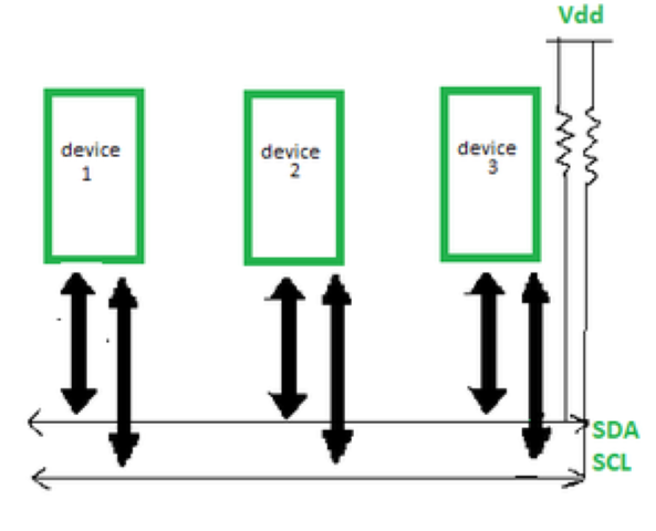
According to I2C protocols, the data line can not change when the clock line is high, it can change only when the clock line is low. The 2 lines are open drain, hence a pull-up resistor is required so that the lines are high since the devices on the I2C bus are active low. The data is transmitted in the form of packets which comprises 9 bits. The sequence of these bits are –
- Start Condition – 1 bit
- Slave Address – 8 bit
- Acknowledge – 1 bit
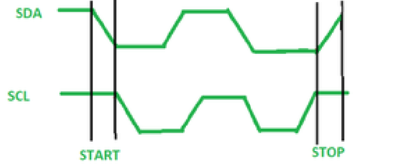
Start and Stop Conditions :
START and STOP can be generated by keeping the SCL line high and changing the level of SDA. To generate START condition the SDA is changed from high to low while keeping the SCL high. To generate STOP condition SDA goes from low to high while keeping the SCL high, as shown in the figure below.
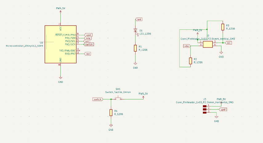
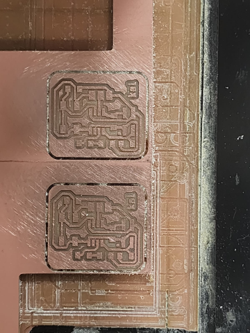
PCB Design
I designed the PCB in Kicad
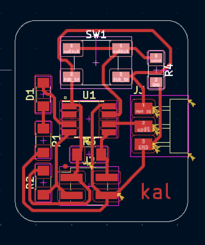
Then I milled the PCB using Modela
Requested the components from inventory
Then I soldered the components
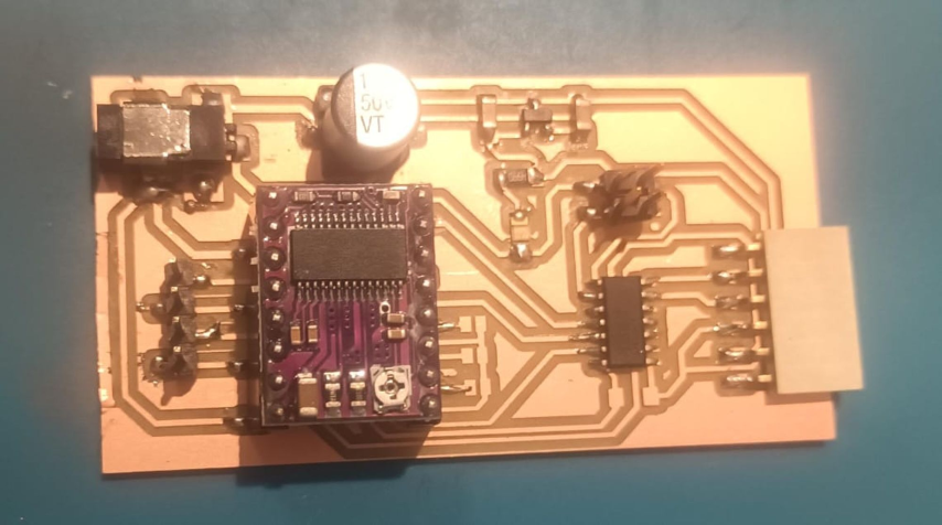
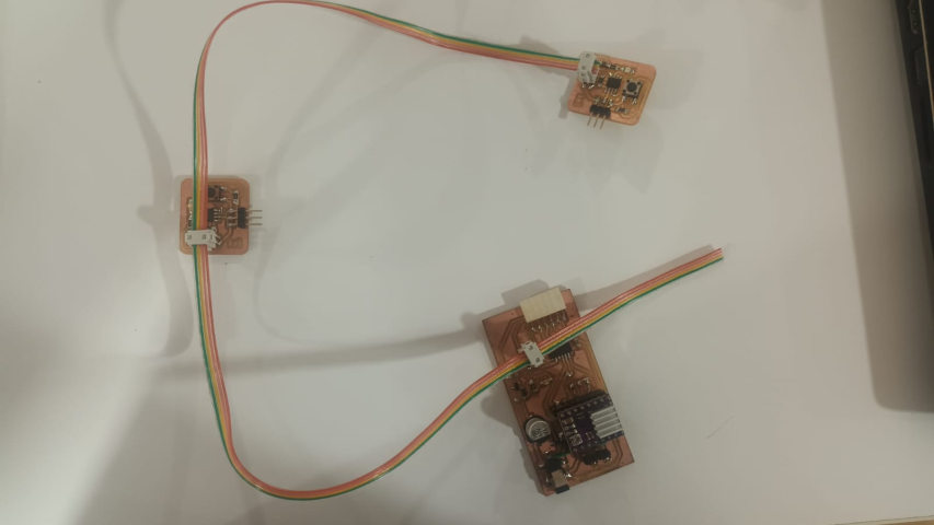
Master PCB
I wanted to use the board I designed on output week as master
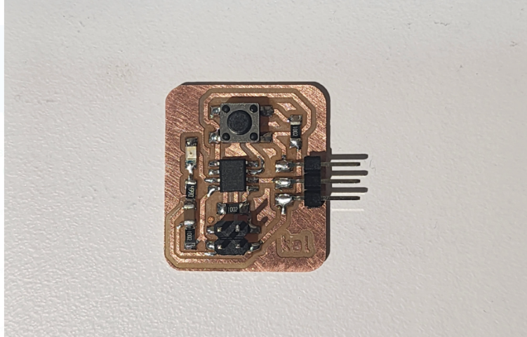
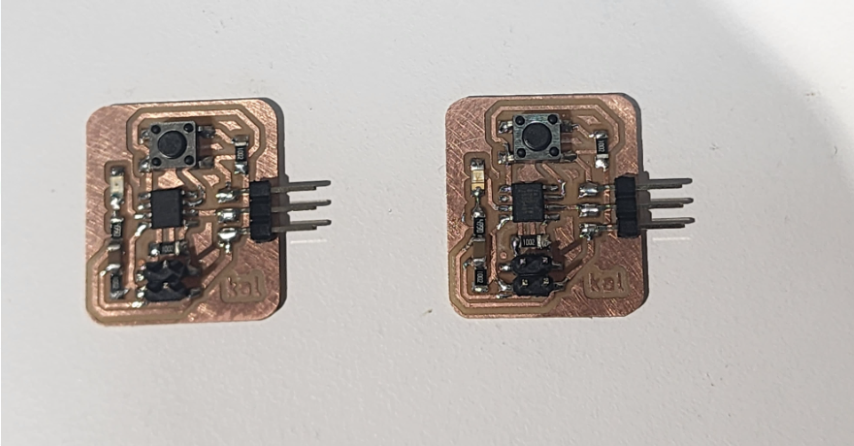
Node PCB
I’m using the board I designed this week as nodes
It looks like this when connected
First I used an example from Arduino IDE to check whether the program can be uploaded
Blink test
void setup() {
  // initialize digital pin LED_BUILTIN as an output.
  pinMode(1, OUTPUT);
}

// the loop function runs over and over again forever
void loop() {
  digitalWrite(1, HIGH);  // turn the LED on (HIGH is the voltage level)
  delay(1000);                      // wait for a second
  digitalWrite(1, LOW);   // turn the LED off by making the voltage LOW
  delay(1000);                      // wait for a second
}
Result
Then I used another code to check serial communication
Hello world
void setup() {
  // Initialize the Serial communication at 9600 baud rate
  Serial.begin(9600);
}

void loop() {
  // Print "Hello, World!" to the Serial Monitor
  Serial.println("Hello, World!");

  // Wait for 1 second
  delay(1000);
}.png)
Then I generated a code using chatgpt for i2c communication protocol
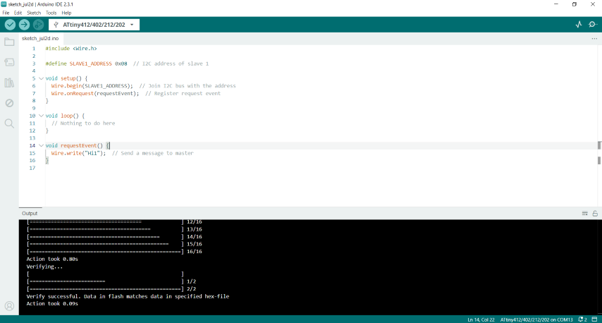
First I uploaded the code to Node 1. I’m planning to name it Ashley
Code for Node 1
#include <Wire.h>

#define SLAVE1_ADDRESS 0x08  // I2C address of slave 1

void setup() {
  Wire.begin(SLAVE1_ADDRESS);  // Join I2C bus with the address
  Wire.onRequest(requestEvent);  // Register request event
}

void loop() {
  // Nothing to do here
}

void requestEvent() {
  Wire.write("Hi1");  // Send a message to master
}
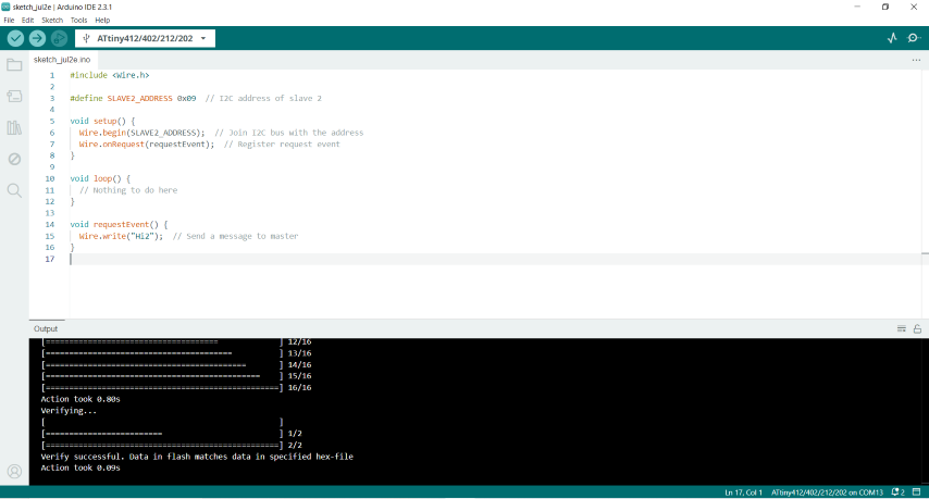
Then I uploaded the code to Node 2 and I’m planning to name it obe
Node 2
#include <Wire.h>

#define SLAVE2_ADDRESS 0x09  // I2C address of slave 2

void setup() {
  Wire.begin(SLAVE2_ADDRESS);  // Join I2C bus with the address
  Wire.onRequest(requestEvent);  // Register request event
}

void loop() {
  // Nothing to do here
}

void requestEvent() {
  Wire.write("Hi2");  // Send a message to master
}
Then I uploaded the code for master
Master code
#include <Wire.h>

#define SLAVE1_ADDRESS 0x08 // I2C address of slave 1
#define SLAVE2_ADDRESS 0x09 // I2C address of slave 2
// Add more slave addresses as needed

void setup() {
  Serial.begin(9600);  // Start serial communication at 9600 baud rate
  Wire.begin();        // Join I2C bus as master
}

void loop() {
  requestDataFromSlave(SLAVE1_ADDRESS);
  requestDataFromSlave(SLAVE2_ADDRESS);
  // Add more requests as needed for additional slaves

  delay(1000);  // Wait for 1 second before requesting data again
}

void requestDataFromSlave(byte address) {
  Wire.requestFrom(address, 2);  // Request 2 bytes from slave

  while (Wire.available()) {  // Slave may send less than requested
    char c = Wire.read();     // Receive a byte as character
    Serial.print(c);          // Print the character
  }
  Serial.println();           // Print a newline character
}
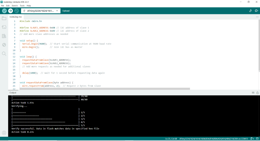
Once all the boards were programmed I checked the serial monitor and noticed that the messages were recieved
Communication
.png)
Modified master code including blink and I also modified the node codes to change the message from Hi to their respective names. Ashley and obe
#include <Wire.h>

#define SLAVE1_ADDRESS 0x08 // I2C address of slave 1
#define SLAVE2_ADDRESS 0x09 // I2C address of slave 2
// Add more slave addresses as needed

void setup() {
  Serial.begin(9600);  // Start serial communication at 9600 baud rate
  Wire.begin();        // Join I2C bus as master
}

void loop() {
  requestDataFromSlave(SLAVE1_ADDRESS);
  requestDataFromSlave(SLAVE2_ADDRESS);
  // Add more requests as needed for additional slaves

  delay(1000);  // Wait for 1 second before requesting data again
}

void requestDataFromSlave(byte address) {
  Wire.requestFrom(address, 5);  // Request 2 bytes from slave

  while (Wire.available()) {  // Slave may send less than requested
    char c = Wire.read();     // Receive a byte as character
    Serial.print(c);          // Print the character
  }
  Serial.println();           // Print a newline character
}.png)
Result
Design files
Node 2 Code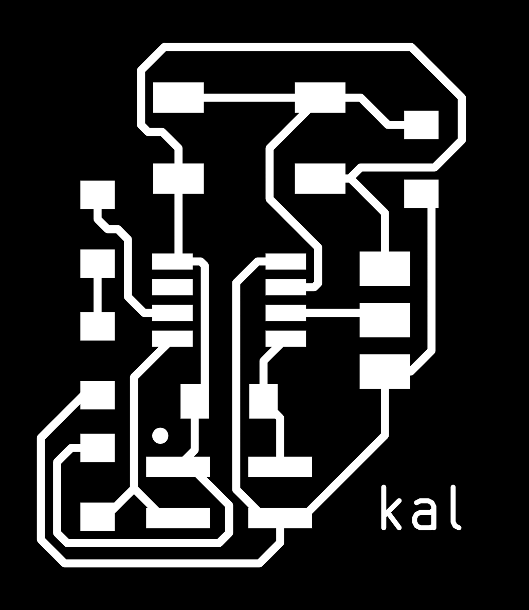
Master Code